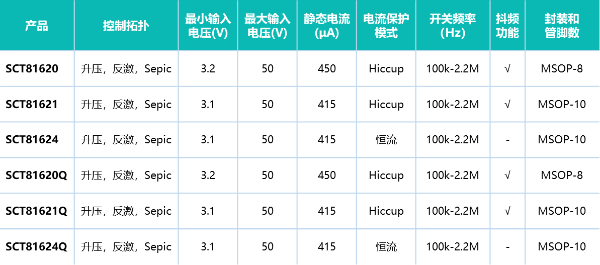
Products


 0
0


BOOST拓扑应用指南
If you have any questions, please contact: wesley-lin@silicontent.com sales@silicontent.com
Abstract
BOOST is one of the three basic topologies in switch-mode power supplies, applied in scenarios where the supply voltage is low but the load requires a higher voltage than the input. Examples include car lights, audio amplifiers, central control systems, T-BOX, lidar, etc.
Due to different voltage and power requirements in various application scenarios, the power and voltage tolerance of integrated MOSFET boost converters can sometimes be limited. Integrated MOSFETs using a single die process tend to be more expensive than mature discrete MOSFETs available on the market, and discrete MOSFETs are more diverse and easier to choose from. However, using a multi-die combined package may limit reliability, heat dissipation, and flexibility.
In such cases, using an external MOSFET with a controller can be a cost-effective choice. The use of external power devices introduces some challenges in component selection for the application. This article will outline the calculation of parameters for the BOOST topology application based on the SCT8162xQ series, specifically the SCT81620.
Example Specifications:
Table of Contents:
Circuit Composition
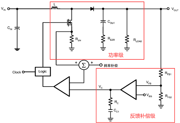
Once the power topology is determined, the power stage parameters affect system efficiency, EMI, and cost.
The device selection process involves first determining the parameters for the power stage components, followed by selecting the compensation network to ensure stable operation and adequate load dynamic response.
Specification Confirmation
SCT81620Q chip input voltage range: 3.2V-50V, which is wider than the required input voltage range of DC6V-16V and voltage tolerance of 36V.
Duty Cycle, Dmax: , with a system efficiency preset at 90%.
The switching frequency is set to 350KHz, which maintains a 91% duty cycle. The maximum duty cycle can be adjusted by changing the switching frequency.
3Calculation of Related Parameters
3.1 Inductor Selection
To avoid core saturation during operation, the peak inductor current should not exceed the inductor's saturation current. The worst-case scenario for a BOOST topology inductor occurs when the load is at full load and at VIN_min. Based on volt-second balance and inductor current ripple, the inductance value can be calculated, with a ripple rate typically chosen between 20%-40%, which provides the best cost-performance ratio. A smaller inductor results in a higher current ripple, necessitating a larger saturation current, which increases the temperature rise of the switching transistor and may cause more EMI issues. Conversely, a larger inductor reduces the current ripple but leads to worse dynamic response, larger size, and potentially higher costs.
The average inductor current, IL = Io / (1 - D) = 1.4 / (1 - 0.876) = 11.29A
The ripple current, △IL, is chosen as 30% of the average current: △IL = 0.3 * IL = 3.39A
The peak inductor current, IPK = IL + △IL / 2 = 12.98A.
Considering a 20% margin, the inductor should have a saturation current of at least ≥16.22A.
The switching frequency, fsw, is preset at 350KHz.
Inductance value: L = (Vin_min * D) / (△IL * fsw) = (6V * 0.876) / (3.339A * 350KHz) = 4.43µH, so the standard value of 4.7µH is selected.
3.2 Current Sensing Resistor Selection
The current sensing resistor in the BOOST topology sets the peak current limit. Considering IPK with a 10% margin, the current limit is set to 14.42A.
Using the equation for peak current sensing: IPEAK_CL = (Vsense - 40µA * RSL * D) / RSNS = 146.5mV / 14.42A = 10.16mΩ
A 10mΩ resistor is initially chosen based on the assumption of no external slope compensation, with RSL = 0Ω. If RSL is not 0Ω, it needs to be factored in.
The resistor is a power-consuming component, so it is important to evaluate whether its rated power is sufficient.
The power dissipation in the resistor is: PRSNS = IPEAK_CL^2 * RSNS = 14.42A * 14.42A * 0.01 = 2.08W, so a 3W, 1% tolerance 2512 package is chosen.
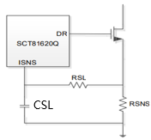
3.3 Current Sampling Blanking and Slope Compensation
Due to parasitic parameters, the switching transistor's switching edges inevitably cause switching noise, which could lead to internal malfunctions. To eliminate the effects of switching noise, sampling delays or external RC filtering circuits are necessary. To prevent subharmonic oscillations under high duty cycles, the SCT81620Q provides internal fixed compensation with an option for external adjustable slope compensation.
If the internal slope compensation is insufficient, external slope compensation using RSL is required. According to peak current mode control theory, the slope of the compensation must be greater than half the rate of decrease of the inductor current, and a value of 0.75 is optimal to prevent subharmonic oscillations under high duty cycles.
Using the equation for slope compensation:
(40µA * RSL + 90mV) * fsw / (((Vo + Vd) - VIN) * RSNS / L) = 0.39 < 0.75
It is recommended to add external slope compensation. Based on the formula, RSL can be selected as 560Ω, and RSNS should be changed to 9mΩ. After adding external slope compensation, the current limit will change, so the selection of the sampling resistor is an iterative process.
When an external RC filter is used, the chip will not respond to overcurrent during the blanking period. The overcurrent protection will be ineffective if the conduction time is less than 2 * RSL * CSL, and this overcurrent point will vary with the supply voltage.
To ensure the complete discharge of CSL during the off period, the RC time constant must meet the condition: 3 * RSL * CSL < (1 - D) / fsw
This gives a maximum value for CSL of 214pF.
From the equation:
(1 - Vin_max / Vo) / fsw > 2 * RSL * CSL
The maximum supply voltage for effective current limiting is calculated as 39.6V.
3.4 MOSFET Selection
MOSFETs are core components in power supplies, and their selection significantly affects system performance and cost. They are also major sources of heat in the system. In automotive applications, which often operate in enclosed environments, considerations for heat dissipation and manufacturing convenience suggest choosing surface-mount packages such as 5mm * 6mm. Aluminum housings can also be used for heat dissipation. Based on common failure modes of MOSFETs in DC/DC applications, it is important to assess avalanche and SOA (safe operating area) ratings. Selecting the appropriate MOSFET specifications is also an iterative process.
Gate Drive Voltage
Since the controller's gate drive voltage is 6V, MOSFETs with a threshold voltage of 4V or below are suitable. Considering the automotive environment, choosing a MOSFET with a 4V threshold improves anti-interference performance.
Drain-Source Voltage Rating
Vds > 1.25 * (Vo + Vd) = 1.25 * (43 + 0.85) = 54.8V, so a 60V rated MOSFET is selected.
Rated Current Range
Id > (3 - 5) * IPEAK_CL = (3 - 5) * 14.42A = 43A - 72A.
Gate Charge (Qg)
At frequencies above 100KHz, parasitic capacitances between the MOSFET's gate, drain, and source generate charge and discharge currents, leading to switching losses. Therefore, it is essential to consider the total gate charge (Qg), output capacitance (Coss), and gate drive resistance when evaluating switching losses. The total gate charge, Qg_total, is a key parameter and should not be large enough to overload the internal VCC regulator. Although the SCT81620 does not have current limiting, power dissipation should be considered.
Qg < 70mA / fsw = 200nF.
Thermal Evaluation
Based on the above steps, the initial choice is the IAUC60N06S5N074 (7.4mΩ @ 60V, 60A). To ensure MOSFET reliability, it is typically recommended to lower the maximum operating junction temperature by 10°C to 25°C. Common FR4 PCB materials have a temperature limit of around 110°C.
Using the selected MOSFET parameters, the current rating after temperature derating is calculated as:
Id(25°C @ Vgs = 6V) = sqrt((Tjmax - Tc) / (Rdson_max * a * Rθjc)) = sqrt((175°C - 25°C) / (11mΩ * 1.62 * 2.9K/W)) = 53.87A.
Id(110°C) = Id(25°C) * (Tj - Tc) / (Tjmax - 25°C) = 53.87A * (150°C - 110°C) / (150°C - 25°C) = 17.2A > IPEAK_CL.
By evaluating MOSFET losses, it is possible to determine whether the thermal resistance of the MOSFET meets heat dissipation requirements. Conduction losses, switching losses, and gate drive losses are the main contributors to total power dissipation. If necessary, additional heat sinks can be used to assist with cooling.
3.5 Freewheeling Diode Selection
In automotive applications, which are typically in enclosed environments with higher temperatures, the selection of freewheeling diodes is critical. In addition to low forward voltage (VF), the diode's reverse leakage current (IR) and package heat dissipation characteristics are essential for reducing the risk of thermal runaway. It is also important to select a diode that can handle the surge current during startup due to the inevitable path between input and output in the BOOST topology.
The reverse voltage rating of the diode must be greater than the load voltage: Vrrm > 1.25 * Vo = 1.25 * 43V = 53.75V, so a 60V-rated diode is chosen.
The freewheeling current, ID = (3 ~ 5) * Io = (3 ~ 5) * 1.4A = 4.2A ~ 7A, and the DIODES PDS760Q is selected.
3.6 Output Capacitor Selection
① Voltage Rating
The voltage rating should be (1.25 - 1.5) * Vo = 1.25 * 43V = 53.75V, so a 63V capacitor is selected.
② Capacitance
Considering load step changes from 10% to 90% (i.e., from 0.14A to 1.26A), the output current is entirely supplied by the output capacitor. To limit the output voltage variation to no more than 5% (2.15V), a sufficiently large output capacitance is required. The BOOST topology transfers energy to the output during Toff, and there is an inherent non-compensable right-half-plane zero. Therefore, the system bandwidth should be set between 1/10 to 1/3 of the right-half-plane zero. For low ESR, MLCC ceramic capacitors are preferred. The capacitor's tolerance and DC bias should be considered.
Right-Half-Plane Zero Frequency:
f_rhpz = (Ro * (1 - D)^2) / (2π * L) = ((43 / 1.4) * (1 - 0.87)^2) / (6.28 * 4.7µH) = 17.58KHz.
From the equation I * ∆T = C * ∆U, where I = ∆Io = 1.12A, ∆T = 0.3 / fc, ∆U = 2.15V:
Cout > 0.3 * ∆Io / (fc * ∆Vo) = 0.3 * 1.12A / (3.516KHz * 2.15V) = 44.44µF.
Thus, four 63V 2220 package 22µF capacitors are selected.
Considering cost and large capacitance, when using electrolytic capacitors, it is important to pay attention to ripple current and ESR. The ESR should be as small as possible, as it affects the bandwidth and phase margin near the zero frequency. For this application, using ceramic capacitors in parallel with electrolytic capacitors improves filtering performance.
3.7 Input Capacitor Selection
The input current in a BOOST topology is continuous. Due to variations in inductor current, the input capacitor charges and discharges, and internal ESR causes voltage ripple. To meet different customer requirements for input voltage ripple, sufficient capacitance should be used to limit input voltage ripple within the specified range, for example, 200mV.
① Voltage Rating
The voltage rating should be (1.25 - 1.5) * VIN_max = 1.25 * 36V = 45V, so a 50V-rated capacitor is chosen.
② Capacitance
For low ESR, ceramic capacitors are preferred. A 10µF 50V MLCC ceramic capacitor is used to meet the ripple current requirements.
3.8 Enable Control Implementation
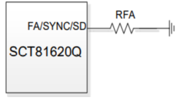
The Enable Pin (SD) is used to turn the chip on and off. The SD pin's maximum voltage rating is 5.5V. Therefore, to avoid accidental operation, a 100KΩ resistor is connected between the SD pin and the input ground, and the shutdown function is active-low.
3.9 Output Voltage Setting
The output voltage is set by a resistive divider connected to the feedback pin, FB. The output voltage is determined by the following equation:
Vout = Vref * (1 + Rtop / Rbot) where Vref = 0.6V.
RTOP=RBOT*(Vo/Vref-1)=24.9K*(43V/1.26V-1)=825KΩ
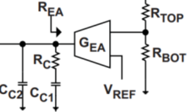
3.10 Compensation Element Parameter Calculation
Since the power stage includes LC components, the loop gain will experience time delays or phase shifts. Therefore, the error amplifier requires frequency-domain gain and phase compensation. The error amplifier of the SCT81620/Q adopts a voltage-controlled current-mode operational amplifier structure and uses peak current mode control.
In the BOOST topology, energy is transferred to the output during Toff, and there is an uncompensated right-half-plane zero, so the system bandwidth, fc, is recommended to be set between 1/10 and 1/3 of the right-half-plane zero.
By setting RC to provide sufficient phase margin, and using the zero-pole cancellation method, CC1 should be selected to place its zero from the compensation network at or slightly above the power stage load pole (the pole generated by the output capacitance and the load's equivalent impedance), typically around 0.1*fc. The calculation for the relevant parameters is as follows:
Compensation Resistor
Rc = (2π * fc * Co * Vo * Vo) / (Gea * 0.24 / Rsns * Vref * Vinmin)
= (6.28 * 3.516KHz * 43V * 43V * 44µF) / (900µs * 0.24 / 9mΩ * 1.26V * 6V) = 9.9kΩ, rounded to 10kΩ.
Compensation Capacitor
CC1 = 1 / (6.28 * 10kΩ * 0.1 * 3516Hz) = 45.28nF, rounded to 47nF.
The high-frequency pole generated by CC2 is used to cancel the ESR zero of the output capacitor. When the output capacitor is ceramic, the ESR zero frequency is much higher than the operating frequency, so CC2 can be omitted. However, if the output capacitor is an electrolytic capacitor, the bandwidth needs to be lower, and the impact of ESR variation with temperature on the loop should be considered.
4 Controller Selection and Recommendation