FEATURES:
Qualified for Automotive Applications
AEC-Q100 Qualified with the Following Results:
- Device Temperature Grade 1: -40°C to 125°C
Ambient Operating Temperature Range
- Device HBM ESD Classification Level H2
- Device CDM ESD Classification Level C3B
Wide Supply Voltage Range: 4.5V - 24V
4A Peak Source Current and 4A Peak Sink Current
Stackable Output for Higher Driving Capability
Negative Input Voltage Capability: Down to -5V
TTL Compatible Input Logic Threshold
Propagation Delay: 13ns
Typical Rising and Falling Times: 8ns
Typical Delay Matching: 1ns
Low Quiescent Current: 55uA
Output Low When Input Floating
Independent Enable Logic for Each Channel
Thermal Shutdown Protection: 170°C
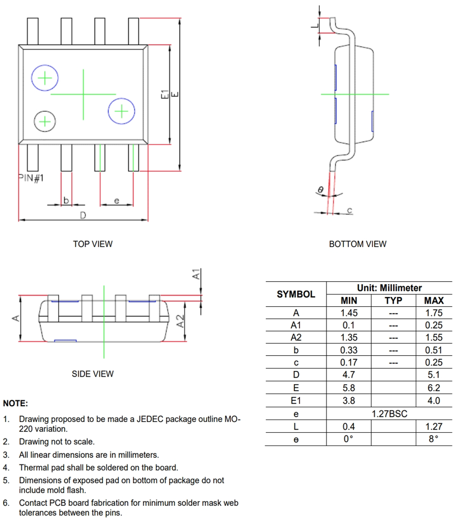
Available in SOP-8 Package
DESCRIPTION:
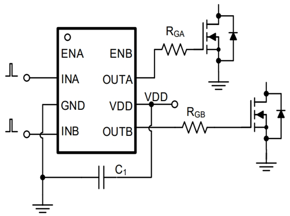
The SCT52240Q is a wide supply, dual channel, high speed, low side gate drivers for both power MOSFET and IGBT. Each channel can source and sink 4A peak current along with rail-to-rail output capability. The 24V power supply rail enhances the driver output ringing endurance during the power device transition.The minimum 13ns input to output propagation delay enables the SCT52240Q suitable for high frequency power converter application. The SCT52240Q features wide input hysteresis that is compatible for TTL low voltage logic. The SCT52240Qhas the capability to handle negative input down to -5V, which increases the input noise immunity. The SCT52240Q has very low quiescent current that reduces the stand-by loss in the power converter. The SCT52240Q each channel driver adopts non-overlap driver design to avoid the shoot-through of output stage. The two channels INA and INB have critical propagation delay matching and artificial dead time implemented in output stage, which enable stackable
output available when the system needs higher driving capability.The SCT52240Q features 170°C thermal shut down. The SCT52240Q is available in SOP-8 package.
APPLICATIONS:
IGBT/MOSFET Gate Driver
Variable Frequency-Drive (VFD)
Switching Power Supply
Motor Control
Solar Power Inverter





 0





 Login Download



 Download datasheet
 Add to Cart
 Collect

