FEATURES:
• Qualified for Automotive Applications
• AEC-Q100 Qualified with the Following Results:
- Device Temperature Grade 1
• Wide Input Voltage Range: 3.5V-36V
• One Synchronous HV Buck Converter VOUT1:
- Up to 3A Continuous Output Current
- Output Voltage Range of 3.3V
• Dual Synchronous LV Buck Converters VOUT2, VOUT3:
- Up to 2A Continuous Output Current
- Output Voltage Range 0.8V to 2.35V with 50mV Steps
• One Synchronous LV Boost Converter VOUT4:
- Up to 500mA Continuous Output Current
- Output Voltage of 5V
• One Load Switch VOUT5:
- Up to 800mA Continuous Output Current
- Output Voltage of 3.3V
• +/- 1.5% Feedback Reference Voltage
• Fixed 2.2MHz Switching Frequency with Integrated Frequency Dither for EMI Mitigation
• FCCM/PFM Selectable
• Sleep mode to save power dissipation
• Programmable Power Sequencer for VOUT2, VOUT3, VOUT4 and VOUT5
• RESETB Output for System Management
• Simple/QA Watchdog
• Integrated Protection Features:
- Hiccup Over Current Protection
- Output Over-voltage/Under-voltage Protection
- Adjustable Input Voltage Under-Voltage Lockout
- Thermal Shutdown Protection
• Functional Safety Features:
- Compliance with ISO26262 Development
- Hardware Integrity up to Support ASIL-B System
- ASIL-B Device Certification by TUV
- BIST
• Up to 1MHz I2C Interface with Optional Packet Error-Checking (PEC)
• Available in QFN-24 (4mm*4mm)
DESCRIPTION:
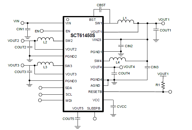
The SCT61450S device is a wide input power management IC with five channels output. The device is designed for SoCs in automotive and industrial radar applications.
The SCT61450S integrates one 3A HV Buck, two identical 2A LV Bucks, one 500mA LV Boost and one 800mA LV Load Switch. Each channel output is continuously monitored, any over-voltage/under-voltage fault will be detected and the device will enter RESET state. All output voltages are pre-programmed, which saves external feedback divider and minimizes system solution. The switching frequency of HV Buck is 2.2MHz/400kHz selectable. The switching frequency is fixed 2.2MHz for LV buck and boost converters. The device features Frequency Spread Spectrum (FSS) with programmable jittering span of the switching frequency and modulation frequency to reduce the conducted EMI.
The device also integrates simple watchdog mode and QA watchdog mode. The dedicated WDI pin allows trigger pulse generated by MCU. Programmable watchdog window is suitable for a wide variety of applications. The RESETB output can be the sequencer of MCU to protect it from device fault.
The SCT61450S device has protection features such as thermal shutdown, short-circuit protection and over-voltage protection. Sleep mode reduces the total supply current to 0.85 mA.
The device has Built-in Self-Test (BIST) Diagnosis over internal analog and digital circuits. All critical comparator and data will be checked during power up stage.
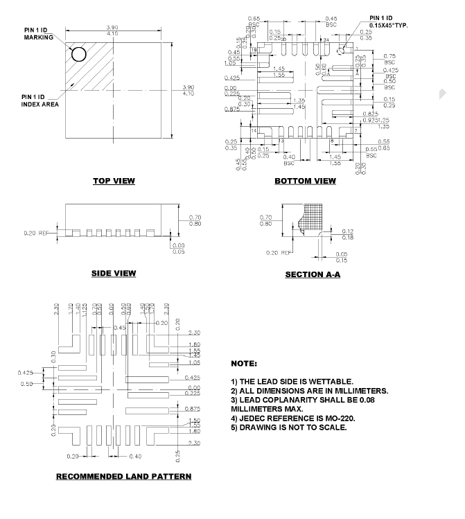
The device is available in a QFN-24(4mm*4mm) package with wettable flanks.
APPLICATIONS:
• ADAS
• 77GHz Radar
• Safety MCU





 0





 Download



 Download datasheet
 Add to Cart
 Collect

