Products


 0
0


With the release of WPC Qi 2.0, Qi 2.0 certification has caught the attention of many wireless charging solution providers and related industries. The launch of Qi 2.0 has injected fresh blood and vitality into wireless charging, bringing countless opportunities and challenges. The convenience and safety of wireless charging are being recognized by users, and the market demand for wireless charging is growing stronger.
What is Wireless Charging?
Wireless charging, simply put, is a technology that allows devices to charge without using conductive wires. It uses principles like electromagnetic induction, electromagnetic resonance, or other technologies that use magnetic fields as a power transmission bridge. The necessary devices are installed at both the transmitting and receiving ends to send and receive the generated alternating current signals, thus completing the charging process.
Mobile phone wireless charging uses the electromagnetic induction method: the primary coil generates alternating current at a certain frequency, which induces a current in the secondary coil via electromagnetic induction, thereby transferring energy from the transmitter to the receiver.
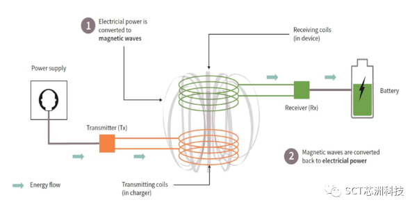
图1 无线充原理图 摘自百度百科
What is Qi 2.0?
Any digital device with the Qi logo can be charged using a Qi wireless charger. Qi 2.0 is an upgraded version of Qi, a newly enhanced wireless charging standard developed by the Wireless Power Consortium (WPC). The charging power of Qi 2.0 has been increased from 7.5W in Qi 1.3 to 15W. Additionally, the existing BPP and EPP protocols have been optimized, forming a new MPP (Magnetic Power Protocol) for better compatibility and higher charging efficiency.
With the release of Qi 2.0, the charging power has been significantly increased, and the maximum input voltage at the transmitting end can reach 19V to reduce current and lower coil losses, thus improving efficiency. This imposes a requirement on the transmitter's ICs to have a voltage rating of ≥19V.
The diagram below shows a transmission-side solution based on the MPP protocol by Silicon Content Technology. The adapter provides 9V voltage, which is stepped up to 9.5-19V by the SCT12A2 to power the full bridge. After security authentication through the authentication IC, and handshaking between the MCU and receiving end, the MCU controls the full bridge to generate alternating current in the coil, which causes changes in the magnetic field to realize electromagnetic conversion and complete wireless charging.
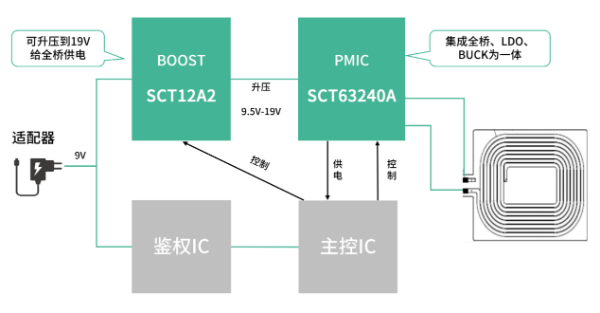
MPP Transmission-side Solution Block Diagram
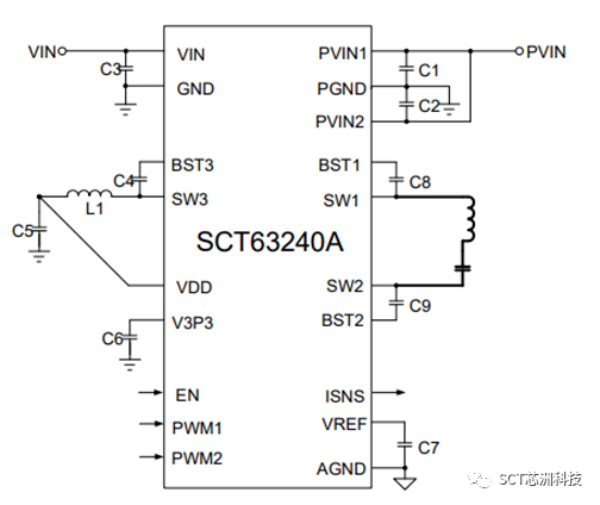
PMIC Solution—SCT63240A
The SCT63240A integrates a full bridge, LDO, and BUCK in one chip. The full bridge has a voltage rating of 20V and a power output of 20W, integrating a 3.3V/200mA LDO and a 5V/1A BUCK. This eliminates the need for an additional LDO to power the MCU, significantly simplifying the TX schematic and reducing both costs and component count.
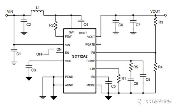
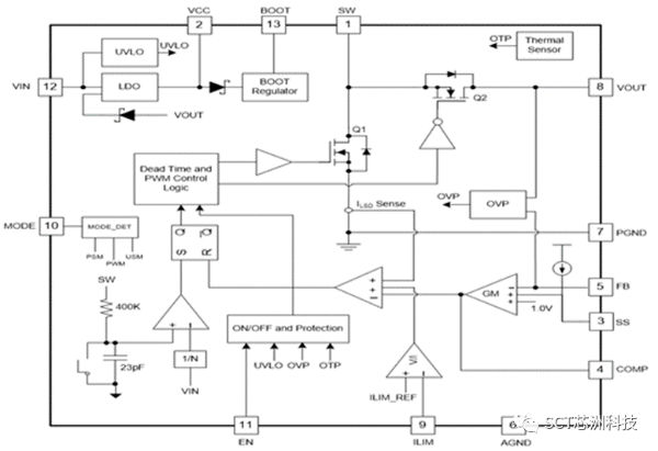
BOOST Solution—SCT12A2
The SCT12A2 is a boost IC capable of outputting up to 21V, with a switch current of 15A and an output power of over 30W, fully meeting the Qi 2.0 requirements. It drives a P-MOSFET for load switching, solving the problem of BOOST ICs not fully shutting down.
BOOST Upgrade Solution—SCT12A5
The SCT12A5 provides significant improvements in efficiency and size:
Currently, both SCT12A2 and SCT63240A have been in stable mass production for over 3 years. Samples for testing are available upon request, and you can contact sales or email to sales@silicontent.com for sample requests or orders.