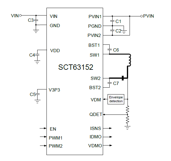
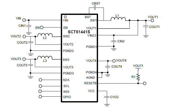
Products


 0
0


With the increasing demand for charging convenience, automotive wireless charging technology has reached a higher level of maturity. Its large-scale application in vehicles avoids the driver's need to search for plugs, differentiate interfaces, and handle charging cables, improving driving safety. In terms of design, it integrates seamlessly with the car interior, being both aesthetically pleasing and practical.
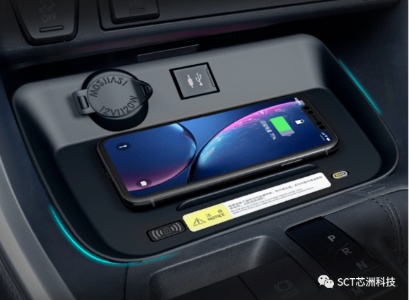
According to monitoring data from the Gaogong Intelligent Automotive Research Institute, the number of new passenger cars in China equipped with wireless charging modules for mobile phones reached 3.5835 million units in 2021, a year-on-year increase of 120.4%, with an installation rate of 17.57%. The installation rate is expected to reach 25% in 2022.
In terms of design, automotive wireless charging typically involves modules such as control chips, magnetic coils, sensors, and power management. When selecting wireless charging modules, it is important to focus on charging efficiency, safety, and compatibility.
Charging Efficiency
Low charging efficiency can impact the user's experience. Therefore, researchers need to pay attention to factors such as the charger’s power, transmission distance, transmission efficiency, and heat loss to improve charging efficiency.
Safety
Considerations such as battery overheating, short circuits, and overcharging are crucial to ensure product safety. Electromagnetic radiation and other issues also need to be addressed to avoid adverse effects.
Compatibility
Different devices have different charging requirements and methods, so compatibility with various brands, models of phones, and other devices must be ensured.
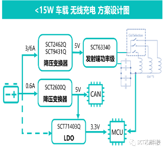
Currently, most automotive wireless charging solutions are based on systems with power output below 15W. This article uses a system solution for 15W or lower to detail the key indicators when selecting power management chips.
In wireless charging applications, the low-dropout pass-through mode for the input power converter is standard. Low-dropout means high efficiency and low EMI.
The SCT2462Q and SCT9431Q are automotive-grade buck converters that support the low-dropout pass-through mode. SCT2462Q can be used for 15W solutions, supporting 6A output and a maximum voltage rating of 42V. It uses second-generation low-dropout pass-through technology, supporting a lower input-output voltage differential (maximum duty cycle of 99.3%), effectively expanding the input voltage range of the wireless charging power transmitter. SCT9431Q can be used for 10W solutions, supporting 3A output and a maximum voltage rating of 42V.
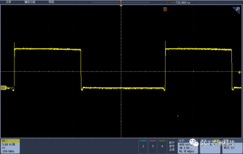
The figure shows the duty cycle of the SCT2462Q, converting from 5V to 5V with a 3A load.
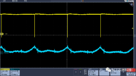
Additionally, SCT's proprietary multi-stage gate driver patent technology can effectively suppress switching node ringing, making it easier to pass relevant EMI tests. Below is a measurement from the SCT2462EVM board. From the waveform, the ringing overshoot when the upper switch is on is only 3.4V at full load, with no multiple oscillations, and the waveform is very clean when turning off.
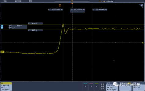
SCT2462EVM: 12V input, 5V/6A full load output, switching node SW waveform (Figure 2 is a detailed view)
Currently, most CAN communication interface devices are powered by 5V, while most MCUs have their supply voltage reduced from 5V to 3.3V. Solutions like SCT2600Q (0.6A buck converter) and SCT71403Q (300mA LDO) can be used.
SCT2600Q is an automotive-grade primary power supply with a maximum input voltage of 60V, supporting a switching frequency of 2.1MHz, which avoids interference with automotive AM (540 KHz – 1600 KHz) bands. It operates in a light-load mode (PSM), greatly improving efficiency in light-load conditions, achieving efficiency above 80% at a 4mA load.
SCT71403Q is an automotive-grade primary LDO with a maximum input voltage of 42V, outputting 3.3V or 5V with a maximum current of 300mA. The standby current is only 2.4uA, and it integrates features like over-current foldback (OCFB), over-temperature protection (OTP), under-voltage lockout (UVLO), and power-good (PG) for voltage and current monitoring and protection, enhancing safety and reliability.
Wireless charging can be divided into three main types: electromagnetic induction, electromagnetic resonance, and radio waves. All three routes have corresponding standards and organizations pushing for market applications and standardization.
Currently, Qi's electromagnetic induction method is the mainstream, and the solutions for both the transmitter and receiver are becoming more refined. Key performance aspects of the transmitter stage include:
3.1 Operating Voltage Range: 3V to 15V
The SCT63340 chip supports an input voltage range of 4.2V to 30V, with the power stage operating within 1V to 26V. It is the chip with the widest input voltage range for 15W wireless charging transmitters.
3.2 Conversion Efficiency
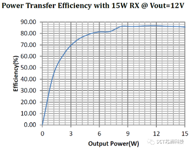
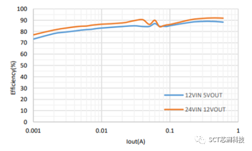
The SCT63340 integrates 13mOhm full-bridge MOSFETs, achieving 86% power transfer efficiency at 15W, which is above the industry average.