Products


 0
0


Buck converters effectively step down higher DC input voltages to lower DC output voltages, providing stable current and voltage output. Both BUCK chips and LDOs are widely used topologies, each fulfilling different roles in various power supply systems due to their unique characteristics.
BUCK chips are preferred by engineers for their high conversion efficiency, especially when outputting larger currents. LDOs (Low Dropout Regulators), on the other hand, support lower dropout voltage conversion with more stable output voltage but are not suitable for large load scenarios.
1. Challenges of BUCK Circuits
As intelligent products continue to emerge in various fields, power supply systems are gradually evolving, and power chips are being developed with wider operating input voltages.
For a fixed output voltage, when the input voltage upper limit increases, using a higher-rated DCDC can solve the issue. However, when the input voltage lower limit requirement becomes lower, BUCK circuits face topological limitations. They need to turn off the upper MOSFET to charge the lower MOSFET’s bootstrap capacitor, which is necessary to maintain the required Vgs voltage for turning on the upper MOSFET.
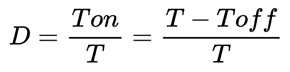
This introduces a maximum duty cycle issue due to the Mini_off time. As shown in the formula below, the larger the Toff, the smaller the duty cycle (D), and the smaller the output voltage (Vout). The maximum duty cycle directly impacts the chip's maximum output voltage.

In this limitation, when the BUCK circuit operates in low-dropout mode, it can cause excessive output voltage drop, poor dynamic response, and large output ripple. At this point, LDOs—designed for low dropout applications—come into play. Integrating the advantages of LDO into BUCK chips, aiming to maximize the duty cycle, is undoubtedly a good solution.
In some scenarios such as battery power and USB power, where the input voltage needs to be just slightly above the output voltage (a few volts), the output voltage cannot be maintained at the set value when the input voltage drops to its lowest point due to the maximum duty cycle limit.
To address this need, SCT has developed an extreme duty cycle control technology that supports near 100% duty cycle operation. In this mode, the chip adapts to reduce the operating frequency and reduce the Mini_off time of the upper MOSFET during a switching cycle, thus increasing the maximum duty cycle. This Low Drop-out Operation, or LDO mode, effectively solves the low-dropout conversion requirements.
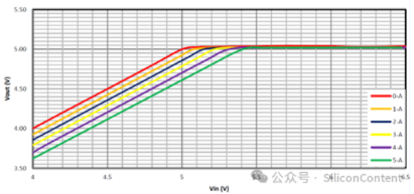
Figure 1: LDO Mode Performance of SCT2450Q
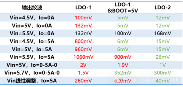
When the SCT2450Q is set to output 5V, the no-load waveform is shown in Figure 2, where the input voltage of 5V can maintain a stable 5V output. The switching frequency drops to 1.6kHz with a ripple of 132mV. As the load increases to 5A, with a constant input voltage of 5V, the switching frequency drops below 1kHz, and the output voltage drops to 4.4V, with a ripple of 960mV.
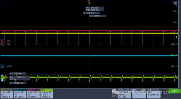
Figure 2: No-load operation with Vin=5V, Vout=5V, Fsw=1.639kHz, Vo_pp=132mV 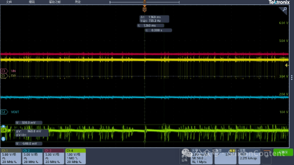
Figure 3: Load operation with Vin=5V, Vout=4.4V, Fsw=735Hz, Vo_pp=960mV
From the above tests, it can be observed that in LDO mode, the switching frequency is pushed to 1kHz to maximize the duty cycle. Under no-load conditions, the duty cycle can reach 100%. However, a new issue arises: inductive ringing, which can be observed from the frequency of the SW pin. When the input voltage is lower, the switching frequency falls below 20kHz, which falls into the audible range, causing the inductive ringing. To address this, the upper MOSFET needs sufficient gate drive voltage to avoid low-frequency switching at the SW pin during turn-off.
The simplest and most effective solution is to add an additional isolated 5V supply to provide power to the BOOT-SW, ensuring that the gate voltage of the upper MOSFET is maintained at 5V, allowing the MOSFET to stay on. In this case, the BUCK chip operates in direct pass-through mode.
However, adding an extra isolated power supply increases board area and cost. An alternative is to use a timer to generate a square wave or have a secondary BUCK operating in CCM mode or light-load FPWM mode to provide a voltage doubler circuit using diodes and capacitors to supply the BOOT-SW and maintain the BOOT voltage.
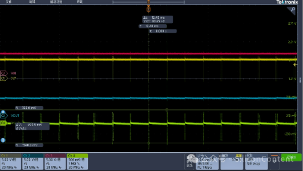
Figure 4: Vin=5.6V, Vout=4.95V, Iout=5A, Vo_pp=900mV 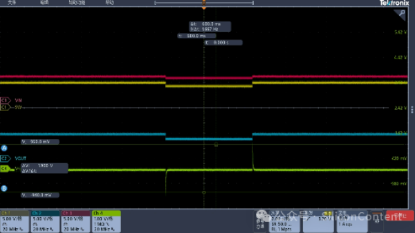
Figure 5: Vin=5V, Iout=0A-5A-0A, Vo_pp=1.9V
Tests were conducted with a timer-generated circuit maintaining a 5V supply to the BOOT-SW. In direct pass-through mode, the output ripple is only 6mV under no load and under load. However, due to the lack of feedback regulation in direct pass-through mode, the ripple can reach 900mV in critical load conditions, and dynamic response ripple reaches up to 1.9V as shown in Figure 5.
Overall, the LDO mode resolves the low-dropout operation challenges for BUCK circuits, but issues still arise when the input voltage is further lowered. Although adding peripheral circuits can solve this, it increases board area and cost.
SCT has developed the second generation of BUCK chips with LDO operating mode. In addition to frequency reduction, the new design limits the minimum operating frequency, avoiding audible noise frequency bands and addressing practical application concerns. The second generation LDO working mode has been added to SCT's 40V family products (e.g., SCT2434Q, SCT2464Q) and 60V family products (e.g., SCT2632B, SCT2630B). Let's take the SCT2464Q as an example to look at the actual performance of the next-generation LDO mode.
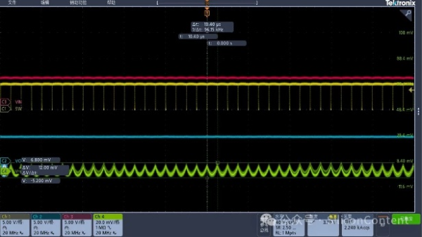
Figure 6: Vin=5V, Vout=4.9V, Fsw=96kHz, Vo_pp=12mV 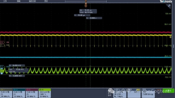
Figure 7: Vin=5V, Vout=4.6V, Fsw=96kHz, Vo_pp=15mV
ith the SCT2464Q set to output 5V, under no-load conditions with an input voltage of 5V, the frequency is 96kHz, and the output ripple is 12mV as shown in Figure 6. Under 5A load conditions, the frequency remains at 96kHz, and the output ripple increases slightly to 15mV as shown in Figure 7.
Additionally, as the load switches from 0A to 5A and back, the dynamic response is significantly improved, with a dynamic response ripple of only 1V as shown in Figure 8.
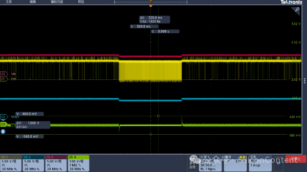
Figure 8: Dynamic response with Vin=5V, Io=0-5-0A
When the input voltage increases beyond 5V, the chip switches from LDO mode to BUCK mode. As the input voltage is reduced back to LDO mode, the output remains stable, with a maximum ripple of only 40mV throughout the transition, as shown in Figure 9.
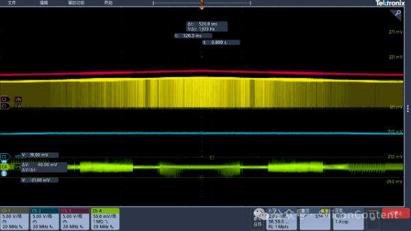
Figure 9: LDO-BUCK-LDO mode switching at 5A load
We have compared the test data for the first-generation LDO mode, first-generation LDO with external BOOT voltage mode, and second-generation LDO mode in the table below, providing a more comprehensive and intuitive view of the technical upgrades and performance improvements for practical applications.
We have compared the test data for the first-generation LDO mode, first-generation LDO with external BOOT voltage mode, and second-generation LDO mode in the table below, providing a more comprehensive and intuitive view of the technical upgrades and performance improvements for practical applications.
In addition to regular BUCK applications, this direct pass-through mode can also be used as an e-fuse function for short-circuit and overcurrent protection.
SCT is committed to the relentless pursuit of power product development, continuously iterating on duty cycle control, EMI optimization, and audio interference suppression technologies to create greater value for customers and provide better services.