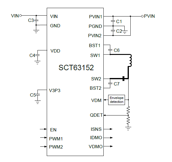
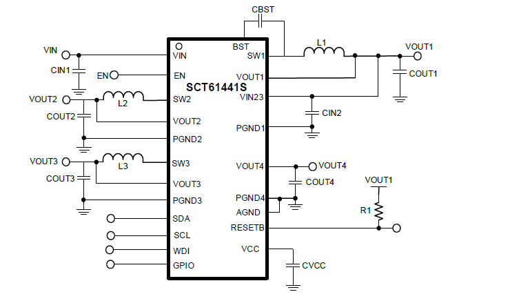
Products


 0
0


In industrial control systems, new energy storage systems, and many electronic devices, to adapt to a wide voltage range and improve energy usage efficiency, many application scenarios require a buck-boost solution for medium-to-high voltage conversion.
For example, in industrial switches using standard POE power supply, a common scenario is stepping down from 48V to ensure stable power delivery. When non-POE power is used, the auxiliary power supply may need to output as low as 9V, and then step up to 12V. Therefore, a buck-boost solution is required. Similarly, outdoor portable storage charging applications need to accommodate solar panels with an output range of 9V-50V and step it down to 12V, which also involves a buck-boost scenario.
Medium-to-high voltage buck-boost modules are typically complex in design and higher in cost. Is such complexity really necessary to meet the requirements?
The mainstream buck-boost topology solutions available in the market include four-switch buck-boost control chips and SEPIC/flyback control chips. In practice, four-switch buck-boost chips are very expensive, and SEPIC/flyback control chips are quite complex to design.
If only buck-boost functionality is required with relatively small power and no isolation needed, this article introduces a cost-effective and simple design for buck-boost solutions using the SCT2650 as an example, to meet the needs of more application scenarios.
The SCT2650 is a buck chip with a 4.5V-60V input and 5A continuous output, integrating an 80mΩ Rdson high-side power MOSFET. The chip uses peak current mode control, and the output voltage is adjustable, featuring excellent transient response for both line and load, which simplifies the external circuit compensation design.
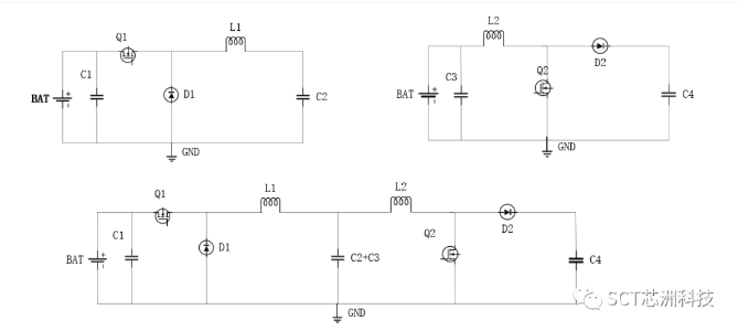
Figure 1: Buck-Boost Cascade Topology Diagram
In the cascade topology shown in Figure 1, buck and boost are combined, and the two power circuits are cascaded to achieve buck-boost functionality. However, at the output of the buck and the input of the boost, the capacitor and inductor form a third-order filter. To maintain the same voltage gain, a lower-order filter can be used instead of the third-order filter, simplifying the original design to a more straightforward buck-boost cascade topology.
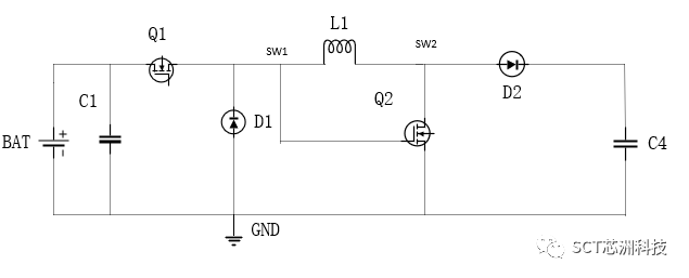
Figure 2 shows the simplified buck-boost cascade topology and also the actual topology used by the SCT2650 to implement the buck-boost function. In the original buck topology, additional components Q2 and D2 are added to implement the buck-boost functionality, transforming the simple buck topology into a buck-boost cascade solution with a single inductor. The control signal for Q2 comes from the SW1 signal of the SCT2650.
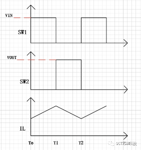
Figure 3: Cascade Buck-Boost Operating Timing Diagram
The control method for this circuit is relatively simple. Between T0-T1, Q1 and Q2 conduct, with SW1 high representing the input voltage, storing energy in the inductor, and discharging the output capacitor to supply the load. Between T1-T2, D1 and D2 conduct, with SW2 high representing the output voltage. The inductor current cannot change abruptly, and the D1 and D2 diodes supply power to the output capacitor and the load. The voltage relationship is derived as follows: By using volt-second balance, we get:

we get:

Thus, the input-output voltage relationship for this topology is:

When the duty cycle changes, this solution can achieve both step-up and step-down functions.
In actual applications, since the SCT2650 has a very wide operating voltage range, the SW1 signal, as the control signal for Q2, may sometimes have a high-level signal that is too high. The maximum gate drive voltage for Q2 is typically around 20V, which could potentially damage the gate. To address this risk, the Q2 drive circuit is further designed.
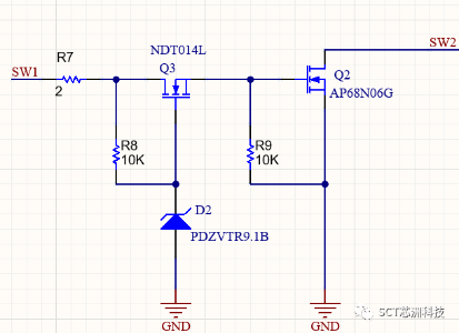
Figure 4: Q2 Drive Circuit Design
A simple voltage regulation circuit is formed by Q3 and a zener diode to limit the maximum drive voltage for Q2 to 9.1V, thus protecting the gate of Q2.
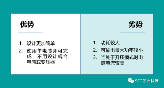
Summary of the Advantages and Disadvantages of Using a Cascade Buck-Boost for Voltage Conversion
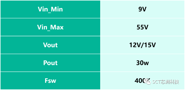
Recommended Application Conditions
SW1, SW2 Waveform and Output Ripple Test Waveforms:

Figure 5: Vin=9V, Vout=12V, Iout=2A
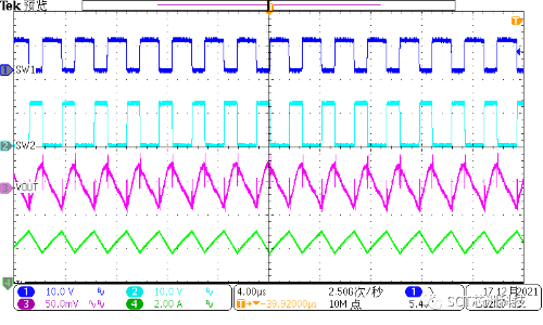
Figure 6: Vin=12V, Vout=12V, Iout=2A
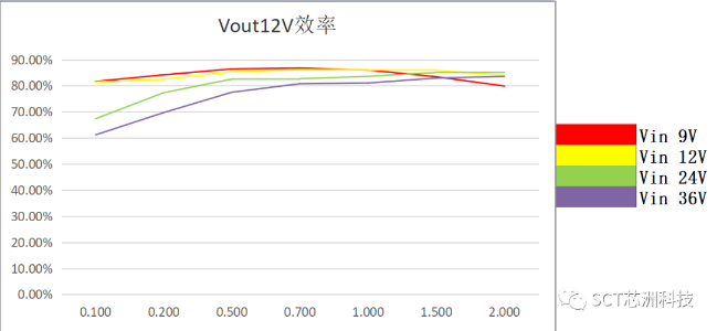
Figure 7: Efficiency Test at Vout=12V