Products


 0
0


Power supply modules play a crucial role in providing power to other functions in system applications. In power supply design, good PCB design can optimize power efficiency, alleviate heat dissipation pressure, reduce noise, and ensure accurate and stable output. Currently, various product applications in industries like industrial, automotive, communication, and consumer electronics all require miniaturization and intelligence, which in turn demands miniaturization of power supply solutions. This article summarizes PCB layout considerations for onboard power supplies, forming a set of recommended layout guidelines for reference.
1. Basic Principles of PCB Layout
1.1 Selection of Power Supply Location
For onboard power supplies, it is important to consider their placement early in the system layout. A key principle is that power supplies should be placed near the load to avoid long PCB traces, which could result in a significant voltage drop between the load side and the power supply's set output voltage, affecting power supply accuracy, dynamic load response, and efficiency. In addition to location, a reasonable estimation of the power supply's area is necessary, or many mandatory PCB layout rules cannot be followed, affecting the power supply's performance.
Moreover, if the system uses a fan for cooling, placing the power supply near the exhaust port helps with heat dissipation, improving power efficiency. To ensure effective fan cooling, the heat dissipation path should be considered to ensure that high passive components (such as inductors, electrolytic capacitors, etc.) do not obstruct the cooling path of shorter active components (such as MOSFETs, PWM controllers, etc.).
1.2 Design of Multi-Layer PCBs
In multi-layer PCB design, it is recommended to add a ground or DC voltage layer as a shielding layer between large current layers (such as input or output voltage layers) and sensitive small signal layers. The ground or DC voltage layer effectively isolates sensitive small signals from the power circuitry, preventing interference. The basic principle for the ground or DC voltage layer layout is to minimize the number of traces and ensure the entire layer is continuous, without being cut. If traces are necessary, they should align with the direction of large current traces to reduce interference.
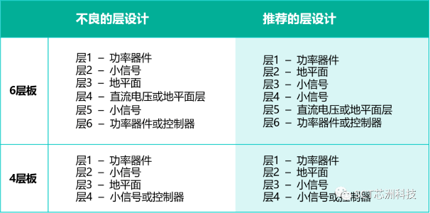
Table 1 Recommended PCB Layer Designs and Poor Designs
In the poor design example in Table 1, the small signal layer is sandwiched between the ground layer and the large current layers, which increases the capacitive coupling between the small signal layer and the large current layers, making the small signal susceptible to interference.
A switch-mode power supply (SMPS) consists of a power circuit and a small signal control circuit. The power circuit includes components that handle large currents, such as inductors, capacitors, and MOSFETs, and these components should be prioritized in layout. The small signal control circuit includes feedback resistors, compensation networks, frequency settings, overcurrent settings, etc., and these components are typically placed in designated positions on the power supply chip.
2.1 Power Trace Width Calculation
Since power traces carry large currents, using a trace width that is too small can lead to increased losses and higher PCB temperatures.
The trace width calculation applies to currents ranging from 1A to 20A, where W is the trace width in mils, I is the current in amperes, and Tcu is the copper weight in oz. For example, with a 5A current and 1 oz copper, the minimum trace width is 120 mils.
The following is an empirical formula for trace width calculation:

2.2 Layout for High Current Rate of Change Circuits
All components and PCB traces have parasitic inductance, capacitance, and resistance. A high current rate of change causes voltage spikes across parasitic inductance, which increases the component voltage rating and introduces noise, reducing the likelihood of passing EMI testing.
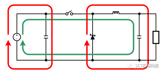
Figure 1 Basic Buck Circuit
Figure 1 shows the basic structure of a buck converter, with current paths drawn for the on and off states of the top MOSFET. The section where only one color is shown is the loop with the high current rate of change, which applies to all circuit topologies.
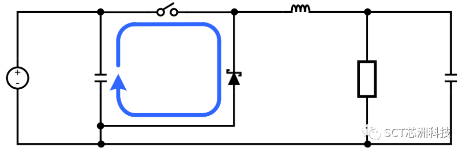
Figure 2 Buck Circuit High Current Rate of Change Loop
As shown in Figure 2, the blue section represents the high current rate of change loop in the buck converter. It is crucial to ensure that the ground for this loop is separated from the ground plane and connected at a single point. The decoupling capacitors in this loop should generally be in the range of 0.1µF to 10µF, using X5R or X7R ceramic capacitors. These capacitors have low parasitic inductance and resistance, providing an ideal current path for high current rate of change currents.
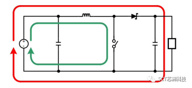
Figure 3 Basic Boost Circuit Structure
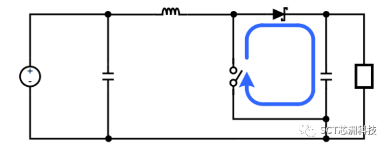
Figure 4 Boost Circuit High Current Rate of Change Loop
Similarly, the same method can be applied to the layout analysis for boost converters, as shown in Figures 3 and 4.
2.3 Layout for High Voltage Rate of Change Nodes
In switch-mode power supplies, the node voltage between the MOS switch and the flyback diode or synchronous rectifier MOSFET switches between ground and high voltage, creating a high voltage rate of change. The ringing voltage at this node is a major source of EMI noise. To prevent noise from coupling into sensitive small signal lines, the area of the switching node should be minimized. However, since this node carries high current, the copper area here is also important for heat dissipation of the MOSFETs and diodes.
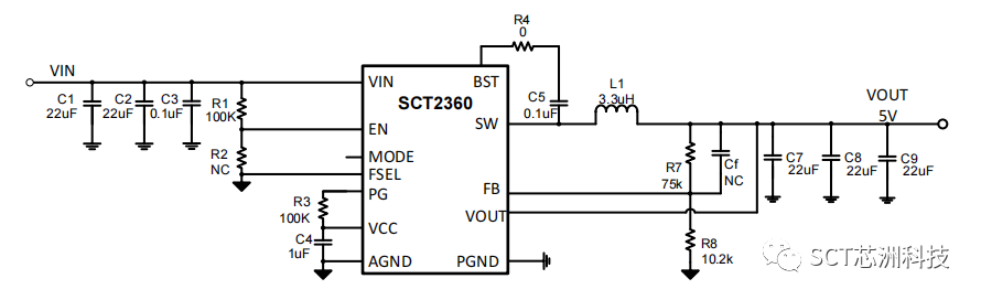
Figure 5 SCT2360 - 12V Input, 5V Output, 6A Load Circuit Diagram
In multi-layer PCB design, it is best to add a ground plane in the layer beneath the switching node to provide additional isolation and prevent noise propagation. For example, in the SCT2360 design, the distance between inductor L1 and SW is small, and the copper area around the SW node should be minimized while still ensuring heat dissipation.
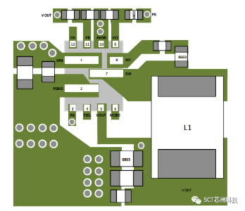
Figure 6 SCT2360 Layout Example
2.4 Layout of High-Frequency Filter Capacitors
High-frequency filter capacitors are crucial components that provide a current path for high current rate of change circuits and play a vital role in reducing voltage stress. For the SCT2360 example, capacitor C3 is placed as close as possible to the chip's VIN and PGND pins, connected via short and thick traces.
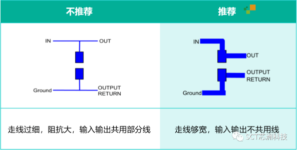
Table 2 High-Frequency Filter Capacitor Layout Example (No Via)
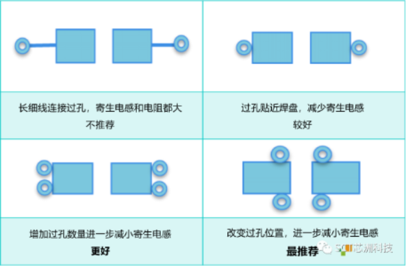
Table 3 High-Frequency Filter Capacitor Layout Example (With Via)
2.5 Layout for Multiple Power Supplies
If multiple power supplies share a common input source and are not synchronized, the input power supply traces should be separated to prevent common-mode noise from propagating through the input and ground, causing mutual interference.
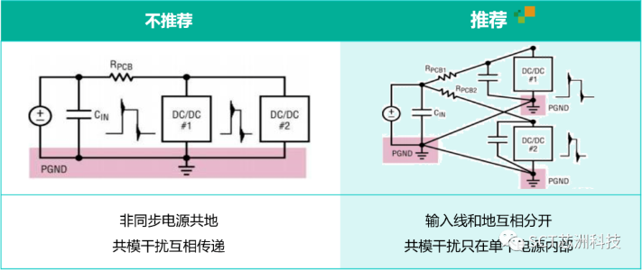
Table 4 Multiple Power Supply Layout Example
80% of power supply design issues stem from PCB layout problems. Investing sufficient time in PCB layout early on can effectively reduce later debugging time and shorten development cycles. SCT23xx series products, with optimized chip PIN configurations, can help customers achieve optimal PCB layouts and the best power performance.
SCT is committed to pursuing the finest details in power chip design and continues to release excellent power chip products to empower customers with the best solutions.