Products


 0
0


Negative voltage power supplies are often used in product design and electronic circuit applications.
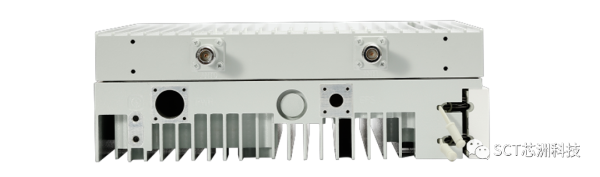
Figure 1: Negative Voltage Power Supply Applied to GaN RF Power Transistors
In common PC power supplies, negative voltage is often used to provide logical judgment levels for serial ports.
In single-board designs, such as operational amplifiers, IGBT drivers, and sensors, negative voltage power supplies may also be required.
In audio equipment, oscillation and feedback circuits require negative voltage to increase dynamic range.
Normally closed GaN (Gallium Nitride) Field-Effect Transistors (RF Power Transistors) also require a dedicated negative voltage power supply.
There are three common methods for generating negative voltage from a positive voltage input:
Using Charge Pump: This method requires fewer external components but has weak load capability, very low output power, and low voltage accuracy.
Using Buck-Boost Circuit: This method has a higher cost.
Using Flyback Circuit: This method requires transformer isolation and reversed output windings, making the design more complex. However, it can provide multiple positive and negative outputs simultaneously, making it suitable when multiple positive and negative power supplies are required.
This article will introduce a solution using a common Buck chip to directly generate negative voltage. It is simple to use, and the load capability of current universal Buck chips can reach tens of amperes, with input voltage ranges covering several volts to hundreds of volts, making it highly versatile.
SCT (SCT24xx series, such as 40V tolerance, 0.6A-6A load capacity) and SCT26xx series (60V tolerance, 0.6A-5A load capacity) chips can achieve positive-to-negative voltage output.
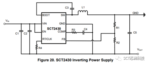
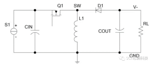
Figure 3: Circuit Diagram of SCT2430
As shown in Figure 3, the negative voltage output and positive voltage output have almost the same number of external components. All components remain in place, and the output of the inductor is connected to ground, creating a new potential. The original ground now serves as the output, resulting in a simple design.
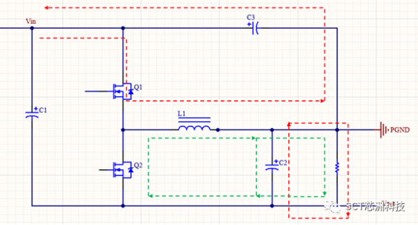
Figure 4: Negative Voltage Output Working State
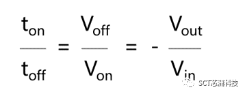
As shown in Figure 4, assuming the voltage drop of Q1 when conducting is VQ1, and the voltage drop of Q2 when conducting is VQ2, during the turn-on (ton) and turn-off (toff) periods of Q1, the voltage across the inductor L1 is as follows:
Von = Vin - VQ1
Vof = -Vout + VQ2
Based on the volt-second balance principle:
Von × ton = Voff × toff,Since the voltage drops of Q1 and Q2 are much smaller than Vin and Vout, the values of VQ1 and VQ2 can be neglected, and the duty cycle D can be derived:
The formula for the duty cycle D is:
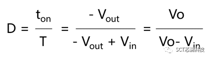
Figure 5: 24V Input to -12V Output, Duty Cycle Around 33%
Thus: :Vo=- Vin×D/(1-D)
As shown in the measurement data, the calculated duty cycle matches the theoretical value.From the above, it can be seen that the absolute value of the output voltage can be greater than or less than the input voltage. Based on the working state diagram, this circuit is no longer working in a buck mode but in a buck-boost mode. Therefore, when designing the external components, load capacity cannot be selected based on the buck circuit parameters.
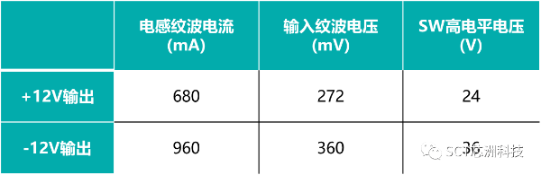
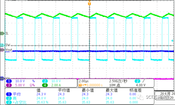
The following shows the SCT2630: Measured data comparison for 24V input, 2A load, +12V and -12V output:
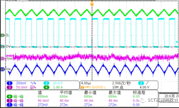
Figure 7: Measured Data for 24V Input, 12V Output
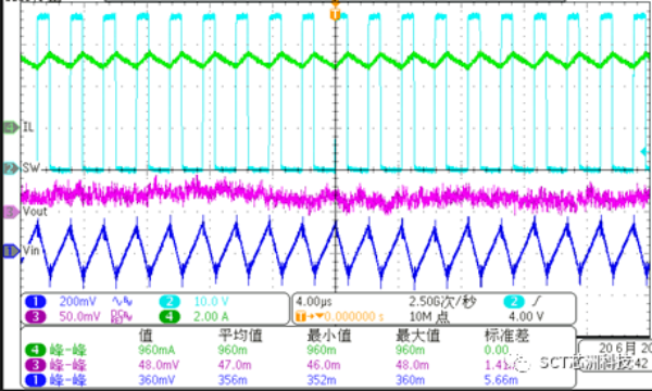
Figure 8: Measured Data for 24V Input, -12V Output
Using a general Buck step-down converter to generate negative voltage is simple and easy to use. It offers a high cost-performance ratio in negative voltage application scenarios, considering the overall cost, performance, and size.
Automotive Solutions:
Car wireless charging power chip integration solutions, focusing on power management, safety, and efficiency.
Automotive-grade power management chips for intelligent cockpits/ADAS/OBC.
Systematic automotive-grade power solutions that balance technological innovation with delivery management, enabling high reliability for new energy vehicles.
Industrial Solutions:
PoE switch power management solutions.
Technical Sharing Solutions:
Alternative solutions for mid-to-high voltage buck-boost conversion.
Summary of power PCB layout considerations.
Introduction to 100V ISO-BUCK isolation application solutions.