Products


 0
0


To cope with complex application environments, switching power supplies integrate multiple protection functions, including overcurrent protection, overtemperature protection, input undervoltage protection, and output overvoltage protection. Overcurrent and overtemperature protection primarily protect the IC, preventing chip burnout. Output overvoltage protection ensures stable output voltage under various application conditions, safeguarding the powered devices from exceeding the maximum voltage they can tolerate.
Due to reasons such as load fluctuations, the power supply may encounter overvoltage situations. The overvoltage amplitude and duration are key factors to consider during power supply design. This article will discuss potential scenarios for output overvoltage and solutions.
PART 1: Output Startup
Impact of No Soft Start
When a switching power supply starts up, the output voltage is initially 0. Without output soft start, the feedback loop will quickly adjust, causing the power supply to charge the output voltage to its maximum output capability. Due to the response speed of the loop, once the output voltage reaches the set value, the duty cycle will take some time to reduce to its normal state (e.g., COMP voltage adjustment in current mode control). During the duty cycle adjustment, overvoltage will occur, and the extent of overvoltage is related to the speed of duty cycle adjustment.
Startup Circuit Implementation
To address this situation, switching power supplies typically design soft start circuits. The soft start circuit allows the output voltage to gradually rise to the set value, thereby preventing output overvoltage.
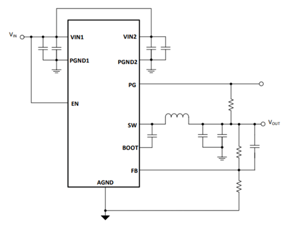
There are various ways to implement soft start circuits. Taking the SCT2432Q buck converter soft start circuit as an example, as shown in Figure 1, the internal feedback error amplifier (EA) introduces SS (soft start voltage) in addition to the feedback voltage FB and reference voltage VREF. The error amplifier compares the lower of FB and the combination of VREF and SS. The SS voltage is generated by charging the external capacitor through an internal constant current source (typically 3uA). Initially, the SS voltage starts at 0 and gradually increases. The feedback voltage FB compares with the SS voltage, causing the FB to follow the SS voltage, thus enabling a linear rise in output voltage.
The SS capacitor can be selected based on factors such as power-up sequencing requirements and output capacitor size to meet system requirements.

Figure 1: Internal Soft Start Logic Block Diagram for SCT2432Q
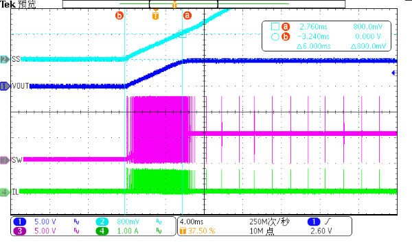
Figure 2: Vout and SS Voltage Proportional Correspondence for SCT2432Q
PART 2: Load Sudden Step Change
Cause of Overvoltage Due to Load Step Change
During the operation of a switching power supply, when the subsequent load is suddenly disconnected or rapidly decreased, the output voltage may experience an overshoot phenomenon. The cause is as follows:
In steady-state operation, the average inductor current is the same as the load current. When the load suddenly decreases, the converter adjusts the duty cycle to reduce the average inductor current. If the load decreases slowly (with the inductor current changing at the same rate as the load), the output voltage will not experience overvoltage. However, when the load decreases faster than the inductor current, the excess energy will accumulate on the output capacitor, causing an overshoot.
Common Methods for Implementing OVP Function
Increasing the loop adjustment speed helps reduce the overvoltage value. When selecting the power supply, models with a COMP pin can be considered. Most power supply chips generally include OVP functionality. Taking the SCT2432Q as an example, it integrates an overvoltage protection comparator. When the feedback voltage (FB) exceeds 110% of the reference voltage (VREF) (response time in microseconds), the overvoltage protection comparator flips, clamping the internal logic, causing the switching transistor to stop oscillating. This prevents energy from being transferred to the output, thus achieving overvoltage protection. However, at this point, the inductor current may not be zero, and some energy may still be released to the downstream, causing the output voltage to continue rising.
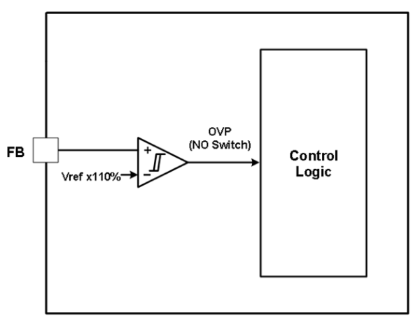
Figure 3: Internal OVP Function Logic Block Diagram for SCT2432Q
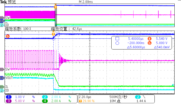
Figure 4: Load Sudden Step Change Overvoltage Protection Function of SCT2432Q
PART 3: Minimum Duty Cycle Limitation
For BUCK and BOOST circuits, the minimum duty cycle is typically limited by the minimum on-time.
Based on the volt-second balance formula, the minimum output voltage under the current input conditions can be calculated. If the set voltage is less than the minimum output voltage, overvoltage will occur. At this point, the OVP function provides protection, and when the output voltage rises to the OVP high threshold, switching will stop, causing the output voltage to decrease. When it drops to the OVP low threshold, operation will resume. In this case, the output voltage behaves more like it is operating in hysteresis mode. This situation typically occurs in high-frequency operation with a small conversion ratio.
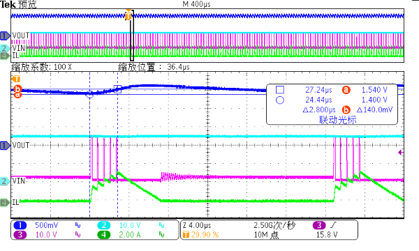
Figure 3: Internal OVP Function Logic Block Diagram for SCT2432Q
PART 4: Significant and Rapid Input Voltage Variation
Overvoltage Caused by Input Voltage Variation
In some complex operating conditions, the input voltage can undergo significant and rapid changes. In automotive applications, the momentary voltage drop during engine startup (waveform reference: ISO 7637-2 PULSE 4) is common. For a buck DC-DC converter, the input voltage drops from the normal value and then quickly recovers.
If the input voltage falls below the output voltage setting value but is still above the undervoltage threshold, the converter will adjust to maximum duty cycle. When the input voltage rapidly recovers to its normal value, due to the duty cycle, the inductor current increases quickly (usually rising to the overcurrent threshold), which causes the output voltage to rise quickly. When the feedback voltage (FB) reaches 110% of the reference voltage (Vref), the OVP (Overvoltage Protection) function is triggered. However, at this point, the inductor current may still have significant residual current, and energy continues to transfer to the output capacitor, causing the output voltage to increase further. This may lead to an output voltage higher than the 110% set value, potentially damaging the downstream load. If the load is light, the output voltage will take longer to return to its normal value.
Solution
To address this issue, Xinzhu Technology's 40V automotive-grade DC-DC converter SCT2434A/CQ optimizes its control method to effectively prevent output overshoot and overvoltage caused by rapid changes in input voltage. This allows for a gradual recovery of the output voltage.
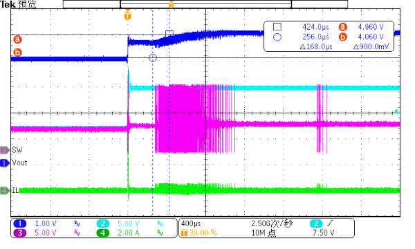
Figure 6: SCT2434CQ Input Voltage Step Change with No Overvoltage Phenomenon Present
(Frequency 2.1M, Inductor 2.2µF, Output Capacitor 44µF)
Overvoltage phenomena in switch-mode power supplies can occur under various conditions, and the above discusses only a few common scenarios.
To address the challenges posed by different situations, Xinzhu Technology will continuously update products and optimize designs to adapt to various demanding applications. With more comprehensive protection functions, covering more complex application scenarios, we aim to improve output voltage stability and provide a safer and more reliable power supply for the load.
SCT2434A/CQ
□ Input Voltage: 3.6-36V
□ Load Capacity: 3A
□ Frequency: 400KHz (AQ) & 2.1MHz (CQ)
□ Built-in 4ms Soft Start
□ 25uA Low Static Current
□ Second Generation LDO Mode
□ 2mm*3mm QFN-12L Package
The SCT2434A/CQ is about to enter mass production. If you need samples for testing or would like to place an order, please contact sales or email us at: sales@silicontent.com.