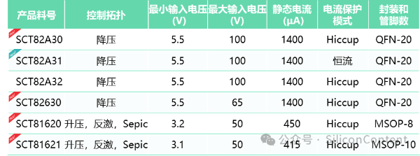
Products


 0
0


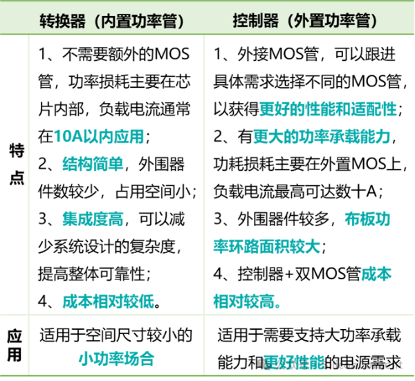
A commonly used DC-DC buck regulator relies on two power switches to perform switching functions. Under the control of a controller, the switches alternate between storing energy in the inductor and releasing it to the load at a specific duty cycle. Buck regulators are typically categorized based on whether the power switches are integrated into the chip or external: Buck converters (integrated power switches) and Buck controllers (external power switches).
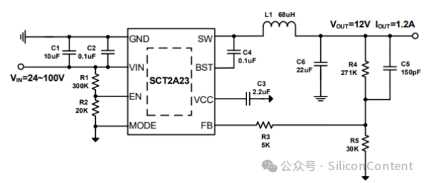
Figure 1: SCT2A23 Buck Circuit
A buck converter, as shown in Figure 1, is composed of an SCT2A23 chip, a power inductor (L1), and input/output capacitors, forming a buck circuit that converts 100V input to 12V output, with the power switches integrated into the chip (HS and LS shown in Figure 2).
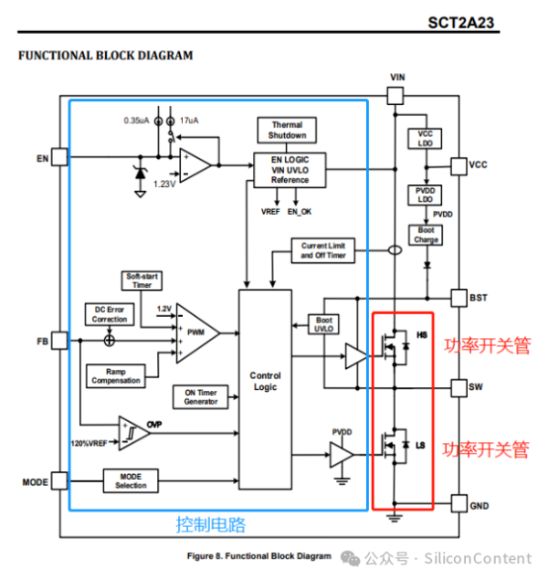
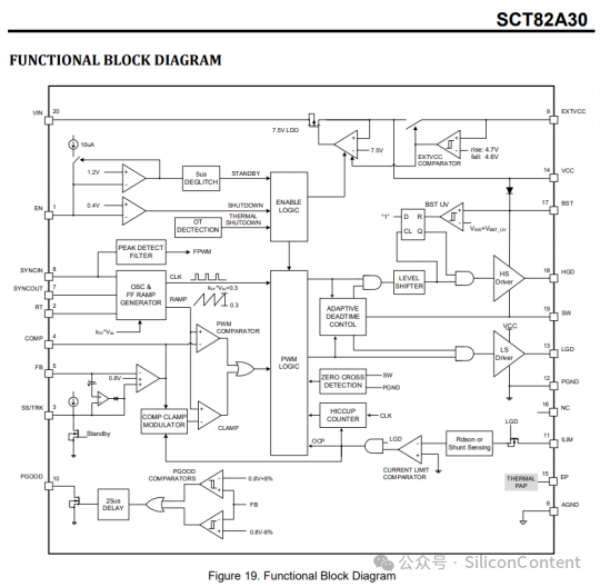
Figure 2: SCT2A23 Chip Block Diagram
In contrast, a buck controller, as shown in Figure 3, lacks integrated power switches.
In Figure 4, the buck controller has only control circuitry and requires external power switches to form a complete buck circuit: the SCT82A30 chip, two power switches (Q1 and Q2), a power inductor (L1), and input/output capacitors, forming a buck circuit that converts 100V input to 5V output.
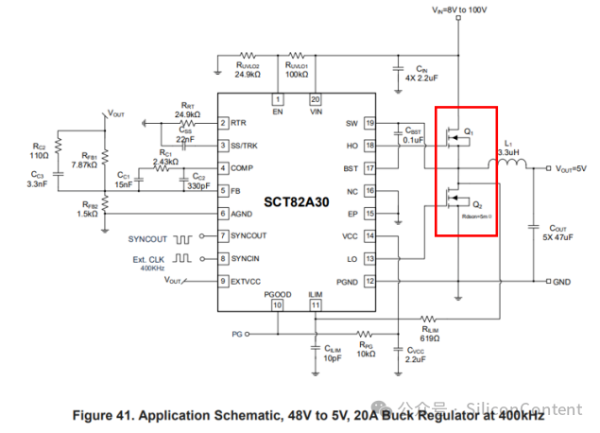
Figure 4: SCT82A30 Buck Circuit
The choice between synchronous buck converters and controllers depends on several factors, such as power requirements, space constraints, and cost control.
In practical applications, converters are mainly used for stepping down high voltage to lower voltage outputs, such as converting 12/24/48V to 5V or 5V to 1.2V/1.8V. In these applications, the lower switch will have a longer conduction time, so it is beneficial to design a lower Rdson for the lower switch to balance the conduction losses and meet most application needs. For example, in the SCT2A23, the upper switch Rdson is 530mΩ, while the lower switch Rdson is 220mΩ.
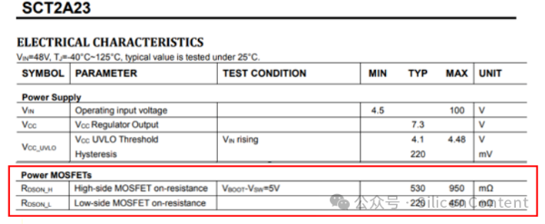
Figure 5: SCT2A23 Parameters
Thus, in some special applications with large duty cycles, the fixed internal MOS may not be able to deliver the nominal maximum current output. A controller, on the other hand, can flexibly select different external MOSFETs to adjust the power loss distribution between the upper and lower switches.
The power MOSFETs act as the valve in the power path of a buck system, carrying the power losses, making the correct selection of these switches crucial for the efficient and stable operation of the power system. This selection requires considering multiple factors such as system efficiency, temperature rise, space constraints, and cost.
The drain-source voltage rating of the MOSFET should be greater than the maximum switching node peak voltage. This must account for the peak voltage at the SW node (VSW_PEAK = VIN_MAX + VNOISE), as shown in the simulation value in Figure 6.
During the initial selection process, a safety margin of 120% of the maximum input voltage (VDS > 120% × VIN_MAX) is typically considered. Noise voltage (VNOISE) is caused by parasitic inductances in the power loop during fast di/dt switching transitions, and can be reduced during debugging by slowing down the turn-on and turn-off rates or adding RC snubber networks, ensuring that VSW_PEAK remains within the safe voltage range for the MOSFET.
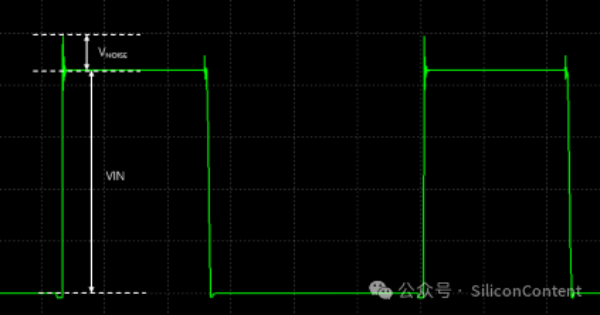
Figure 6: Switch Node Voltage Spike
To determine whether a MOSFET is suitable for a specific application, its power losses and temperature rise must be calculated. The total power loss on the MOSFET (PTotal) is the sum of conduction losses (PCON) and switching losses (PSW).
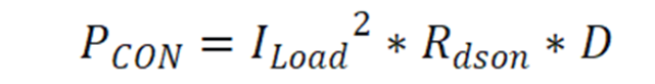
Conduction losses (PCON) can be calculated using Ohm's law, with D representing the duty cycle:
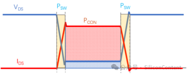
Figure 7: MOSFET Power Loss Components
Conduction losses (PCON) can be calculated using Ohm's law, with D representing the duty cycle: (1)
The switching losses are determined by the turn-on and turn-off processes, where the action takes place at the valley and peak currents of the inductor: (2)
![]()
The switching process, shown in Figure 8, involves energy loss during the rapid voltage-current transitions, from the gate voltage rising to the threshold voltage (VGS_th) and through the Miller plateau, as well as the time taken for the gate voltage to drop back down to the threshold voltage.
The times tr and tf are related to the internal drive parameters of the controller and the characteristics of the external MOSFET, and can be approximated using the charge formula:
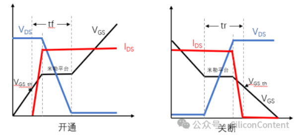
Figure 8: MOSFET Switching On and Off Process
The gate charge (Qg), turn-on threshold voltage (VGS_th), the on-resistance (RON_H and RON_L) of the gate driver, and the supply voltage (VDD) all significantly influence switching losses during fast switching. (3)
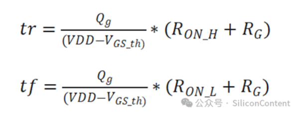
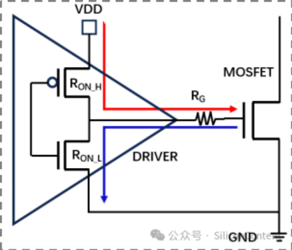
Figure 9: Controller Drive MOSFET Driver Loop
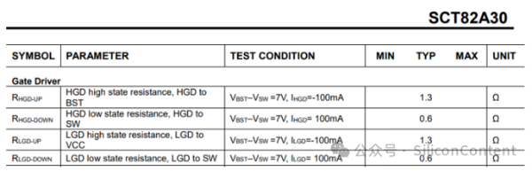
In the formula, RG is the external driving resistor in series with the MOSFET gate at the controller’s drive terminal. RON_H and RON_L represent the internal on-resistance (source-drain resistance) of the controller’s drive terminal. These values are listed in the Gate Driver section of the electrical performance table for the SCT82A30 controller.
Therefore, the total gate charge Qg, the threshold voltage VGS_th, the internal source-drain impedance RON of the driver, and the drive voltage VDD all significantly affect the switching loss of the MOSFET during high-speed switching.
The switching transient losses of the low-side MOSFET mainly arise from the freewheeling loss of the body diode during dead-time. The loss value PSW_L can be determined by equation (4).
![]()
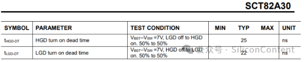
Where tLGD_DT and tHGD_DT are the dead-time durations when the upper and lower MOSFETs are conducting. According to the datasheet, these values are 25ns for tLGD_DT and 22ns for tHGD_DT.
In addition to loss, thermal evaluation of the device is required to preliminarily assess whether the selected MOSFET's junction temperature meets the requirements, ensuring that the junction temperature stays within a safe margin. Different thermal characteristics (thermal resistance) describe the impedance of heat generated by losses as it propagates through various paths (as shown in Figure 10).
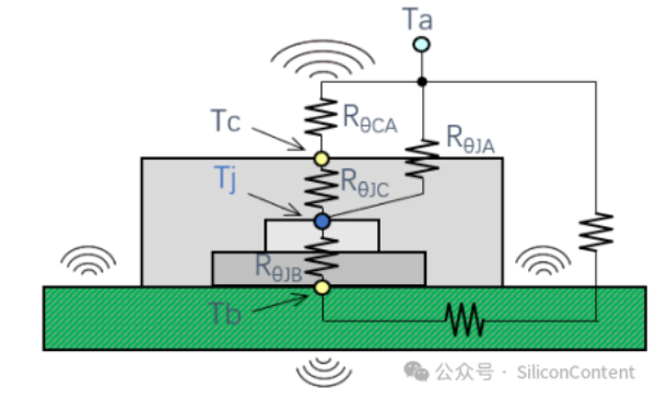
Figure 10: Thermal Transfer Path of Package Device
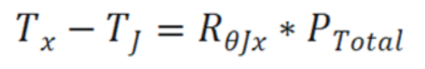
The temperature difference (ΔT) between two nodes is calculated as the thermal resistance (Rθ) between those points multiplied by the total power loss (PTotal) in the device:
ΔT = Rθ × PTotal
For initial evaluation, the thermal resistance values RθJA (junction-to-ambient thermal path) and RθJC (junction-to-case center thermal path) are typically used (5).
More Products:
The SCT82A30 is a 5.5V to 100V input synchronous buck controller capable of driving external MOSFETs with up to 2.3A and 3.5A gate drive current, reducing the need for strict specifications on external MOSFET parameters. It offers an internal 7.5V regulator to drive external MOSFETs in a reasonable linear region.
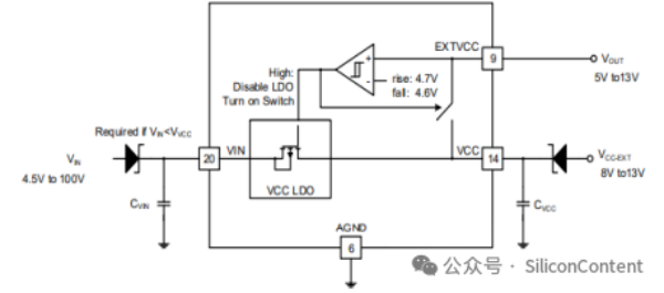
Figure 11: External Power Supply VCC Illustration
The chip supports two external power supply options for the VCC, reducing internal LDO power dissipation at high input voltages, improving efficiency and reducing heat. When EXT_VCC exceeds 4.7V, the internal LDO is turned off and switched to the external VCC, offering up to a 13% efficiency improvement in applications like 48V/72V, as shown in Figure 12.
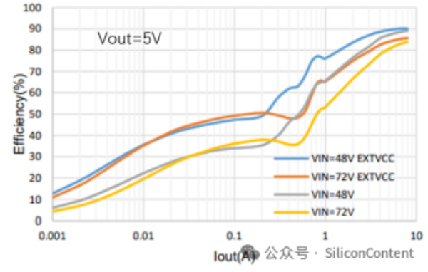
Figure 12: Efficiency Difference of External Power Supply for SCT82A30
For more information on buck controller selection and product details, please visit the official website of SCT and we look forward to further discussions.